 | –≠–ª–µ–∫—Ç—Ä–æ–Ω–Ω—ã–π –∫–æ–º–ø–æ–Ω–µ–Ω—Ç: ST485CN | –°–∫–∞—á–∞—Ç—å:  PDF PDF  ZIP ZIP |
March 2006
Rev 12
1/19
19
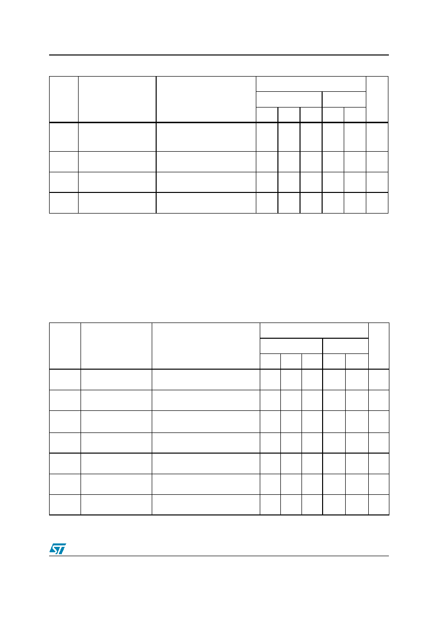
Order code
Part number
Temperature range
Package
Comments
ST485CN
0 to 70 ∞C
DIP-8
50parts per tube / 40tube per box
ST485BN
-40 to 85 ∞C
DIP-8
50parts per tube / 40tube per box
ST485XN
-55 to 125 ∞C
DIP-8
50parts per tube / 40tube per box
ST485CD
0 to 70 ∞C
SO-8 (Tube)
100parts per tube / 20tube per box
ST485BD
-40 to 85 ∞C
SO-8 (Tube)
100parts per tube / 20tube per box
ST485CDR
0 to 70 ∞C
SO-8 (Tape & reel)
2500 parts per reel
ST485BDR
-40 to 85 ∞C
SO-8 (Tape & reel)
2500 parts per reel
ST485XDR
-55 to 125 ∞C
SO-8 (Tape & reel)
2500 parts per reel
ST485
Low power
RS-485/RS-422 transceiver
General features
I
Low quiescent current: 300mA
I
Designed for RS-485 interface application
I
-7V to 12V common mode input voltage range
I
Driver maintains high impedance in 3-state or
with the power OFF
I
70mV tipycal input hysteresis
I
30ns propagation delay, 5ns skew
I
Operate from a single 5V supply
I
Current limiting and thermal shutdown for
driver overload protection
I
Allows up to 64 transceivers on the bus
Description
The ST485 is al low power transceiver for RS-485
and RS-422 communication. Each part contains
one driver and one receiver.
This transceiver draw 300mA (typ.) of supply
current when unloaded or fully loaded with
disabled drivers.
It operates from a single 5V supply.
Driver is short-circuit current limited and is
protected against excessive power dissipation by
thermal shutdown circuitry that placed the driver
outputs into a high-impedance state.
The ST485 is designed for bi-directional data
communications on multipoint bus transmission
line (half-duplex applciations).
The ST485 is available in three temperature
range: commercial (0∞C to 70∞C), industrial (-
40∞C to 850∞C) and automotive (-55∞C to 125∞C)
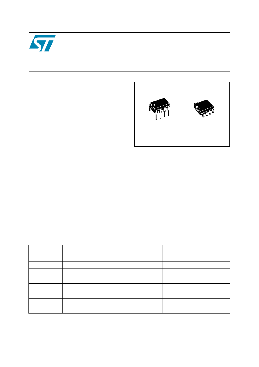
DIP-8
SO-8
www.st.com

Contents
ST485
2/19
Contents
1
Pin configuration . . . . . . . . . . . . . . . . . . . . . . . . . . . . . . . . . . . . . . . . . . . . 3
1.1
Pin description . . . . . . . . . . . . . . . . . . . . . . . . . . . . . . . . . . . . . . . . . . . . . . 3
2
Truth tables . . . . . . . . . . . . . . . . . . . . . . . . . . . . . . . . . . . . . . . . . . . . . . . . 4
3
Maximum ratings . . . . . . . . . . . . . . . . . . . . . . . . . . . . . . . . . . . . . . . . . . . . 5
4
Electrical characteristics . . . . . . . . . . . . . . . . . . . . . . . . . . . . . . . . . . . . . 6
4.1
Driver switching characteristics . . . . . . . . . . . . . . . . . . . . . . . . . . . . . . . . . 7
4.2
Receiver switching characteristics . . . . . . . . . . . . . . . . . . . . . . . . . . . . . . . 8
5
Test circuit and typical characteristics . . . . . . . . . . . . . . . . . . . . . . . . . . 9
6
Package mechanical data . . . . . . . . . . . . . . . . . . . . . . . . . . . . . . . . . . . . 14
7
Revision history . . . . . . . . . . . . . . . . . . . . . . . . . . . . . . . . . . . . . . . . . . . 18
ST485
Pin configuration
3/19
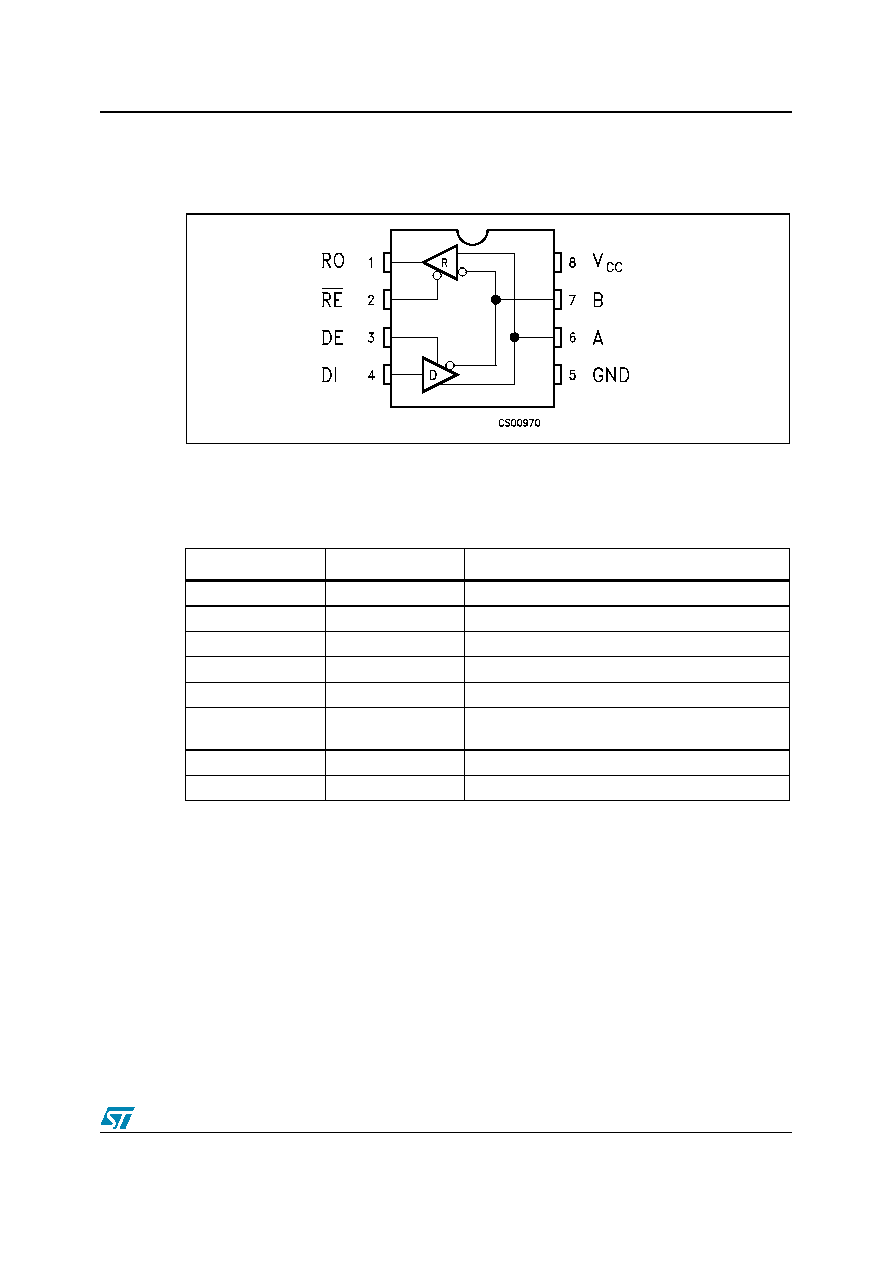
1 Pin
configuration
Figure 1.
Pin configuration
1.1 Pin
description
Table 1.
Pin description
Pin n∞
Symbol
Name and function
1
RO
Receiver Output
2
RE
Receiver Output Enable
3
DE
Driver Output Enable
4
DI
Driver Input
5
GND
Ground
6
A
Non-inverting Receiver Input and Non-inverting
Driver Output
7
B
Inverting Receiver Input and Inverting Driver Output
8
V
CC
Supply Voltage
Truth tables
ST485
4/19
2 Truth
tables
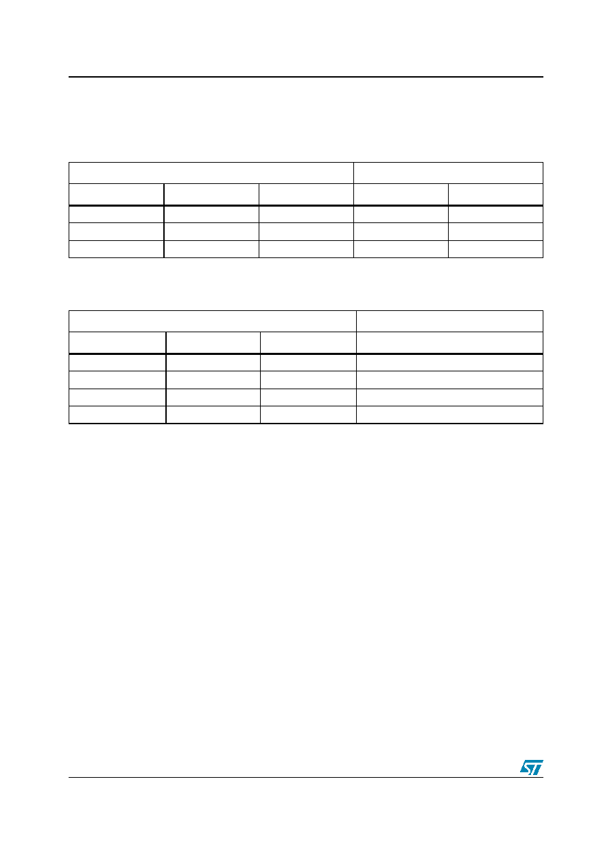
Note:
X = Don't care; Z = High impedance
Note:
X = Don't care; Z = High impedance
Table 2.
Truth table (driver)
Inputs
Outputs
RE
DE
DI
B
A
X
H
H
L
H
X
H
L
H
L
X
L
X
Z
Z
Table 3.
Truth table (receiver)
Inputs
Outputs
RE
DE
A-B
RO
L
L
+0.2V
H
L
L
-0.2V
L
L
L
INPUTS OPEN
H
H
L
X
Z

ST485
Maximum ratings
5/19
3 Maximum
ratings
Note:
Absolute maximum ratings are those values beyond which damage to the device may occur.
Functional operation under these condition is not implied. V+ and V- can have a maximum
magnitude of +7V, but their absolute addition can not exceed 13 V.
Table 4.
Absolute maximum ratings
Symbol
Parameter
Value
Unit
V
CC
Supply Voltage
7
V
V
I
Control Input Voltage (RE, DE)
-0.5 to (V
CC
+ 0.5)
V
V
DI
Driver Input Voltage (DI)
-0.5 to (V
CC
+ 0.5)
V
V
DO
Driver Output Voltage (A, B)
±
14
V
V
RI
Receiver Input Voltage (A, B)
±
14
V
V
RO
Receiver Output Voltage (RO)
-0.5 to (V
CC
+ 0.5)
V
Electrical characteristics
ST485
6/19
4 Electrical
characteristics
V
CC
= 5V ± 5%, T
A
= T
MIN
to T
MAX
, unless otherwise specified. Typical values are referred
to T
A
= 25∞C)
Table 5.
DC Electrical characteristics
Symbol
Parameter
Test conditions
(1)
Value
Unit
-40 to 85 ∞C
-55 to 125 ∞C
Min Typ Max Min Max
V
OD1
Differential Driver Output
(No Load)
5
5
V
V
OD2
Differential Driver Output
(With Load)
R
L
= 27
(RS-485) (
Figure 2.
)
R
L
= 50
(RS-422) (
Figure 2.
)
1.5
5
5
1.4
5
5
V
V
V
OD
Change in Magnitude of
Driver Differential Output
Voltage for
Complementary Output
States
R
L
= 27
or 50
(
Figure 2.
)
0.2
0.2
V
V
OC
Driver Common-Mode
Output Voltage
R
L
= 27
or 50
(
Figure 2.
)
3
3
V
V
OC
Change in Magnitude of
Driver Common-Mode
Output Voltage for
Complementary Output
States
R
L
= 27
or 50
(
Figure 2.
)
0.2
0.2
V
V
IH
Input High Voltage
RE, DE, DI
2.0
2.0
V
V
IL
Input Low Voltage
RE, DE, DI
0.8
0.8
V
I
IN1
Input Current
RE, DE, DI
±
2
±
2
µ
A
I
IN2
Input Current (A, B)
V
CM
= 0V or 5.25VV
DE
= 0V
V
IN
= 12V
V
IN
= -7V
1
-0.8
1
-0.8
mA
mA
V
TH
Receiver Differential
Threshold Voltage
V
CM
= -7 to 12V
-0.2
0.2
-0.2
0.2
V
V
TH
Receiver Input
Hysteresis
V
CM
= 0V
70
mV
V
OH
Receiver Output High
Voltage
I
O
= -4mAV
ID
= 200mV
3.5
3.4
V
V
OL
Receiver Output Low
Voltage
I
O
= 4mAV
ID
= -200mV
0.4
0.55
V
I
OZR
3-State (High
Impedance) Output
Current at Receiver
V
O
= 0.4 to 2.4V
±
1
±
1
µ
A
R
IN
Receiver Input
Resistance
V
CM
= -7 to 12V
24
24
KW
ST485
Electrical characteristics
7/19
4.1
Driver switching characteristics
V
CC
= 5V
±
5%, T
A
= T
MIN
to T
MAX
, unless otherwise specified. Typical values are referred
to T
A
= 25∞C
I
CC
No Load Supply Current
(2)
V
RE
= 0V or V
CC
V
DE
= V
CC
V
DE
= 0V
400
300
900
500
900
500
µ
A
µ
A
I
OSD1
Driver Short-Circuit
Current, V
O
=High
V
O
= -7 to 12V
(3)
35
250
35
250
mA
I
OSD2
Driver Short-Circuit
Current, V
O
=Low
V
O
= -7 to 12V
(3)
35
250
35
250
mA
I
OSR
Receiver Short-Circuit
Current
V
O
= 0V to V
CC
7
95
7
95
mA
1.
All currents into device pins are positive; all cuttents out of device pins are negative; all voltages are referenced to device
ground unless specified.
2.
Supply current specification is valid for loaded transmitters when V
DE
= 0V
3.
Applies to peak current. See typical Operating Characteristics.
Table 5.
DC Electrical characteristics
Symbol
Parameter
Test conditions
(1)
Value
Unit
-40 to 85 ∞C
-55 to 125 ∞C
Min Typ Max Min Max
Table 6.
Driver switching characteristics
Symbol
Parameter
Test conditions
(1)
Value
Unit
-40 to 85 ∞C
-55 to 125∞C
Min.
Typ.
Max.
Min.
Max.
t
PLH
t
PHL
Propagation Delay
Input to Output
R
DIFF
= 54
C
L1
= C
L2
= 100pF
(See
Figure 4.
and
Figure 6.
)
10
30
60
70
ns
t
SK
Output Skew to Output
R
DIFF
= 54
C
L1
= C
L2
= 100pF
(See
Figure 4.
and
Figure 6.
)
5
10
10
ns
t
TLH
t
THL
Rise or Fall Time
R
DIFF
= 54
C
L1
= C
L2
= 100pF
(See
Figure 4.
and
Figure 6.
)
3
15
40
3
45
ns
t
PZH
Output Enable Time
C
L
= 100pFS2 = Closed
(See
Figure 5.
and
Figure 7.
)
70
90
90
ns
t
PZL
Output Enable Time
C
L
= 100pFS1 = Closed
(See
Figure 5.
and
Figure 7.
)
70
90
90
ns
t
PLZ
Output Disable Time
C
L
= 15pFS1 = Closed
(See
Figure 5.
and
Figure 7.
)
70
90
90
ns
t
PHZ
Output Disable Time
C
L
= 15pFS2 = Closed
(See
Figure 5.
and
Figure 7.
)
70
90
90
ns
1.
All currents into device pins are positive; all cuttents out of device pins are negative; all voltages are referenced to device
ground unless specified.
Electrical characteristics
ST485
8/19
4.2
Receiver switching characteristics
V
CC
= 5V
±
5%, T
A
= T
MIN
to T
MAX
, unless otherwise specified. Typical values are referred
to T
A
= 25∞C)
Table 7.
Receiver switching characteristics
Symbol
Parameter
Test conditions
(1)
Value
Unit
-40 to 85 ∞C
-55 to 125∞C
Min.
Typ.
Max.
Min.
Max.
t
PLH
t
PHL
Propagation Delay Input
to Output
R
DIFF
= 54
C
L1
= C
L2
= 100pF
(See
Figure 4.
and
Figure 8.
)
20
130
210
230
ns
t
SKD
Differential Receiver
Skew
R
DIFF
= 54
C
L1
= C
L2
= 100pF
(See
Figure 4.
and
Figure 8.
)
13
ns
t
PZH
Output Enable Time
C
RL
= 15pFS1 = Closed
(See Fig. 2 and
Figure 9.
)
20
50
56
ns
t
PZL
Output Enable Time
C
RL
= 15pFS2 = Closed
(See Fig. 2 and
Figure 9.
)
20
50
56
ns
t
PLZ
Output Disable Time
C
RL
= 15pFS1 = Closed
(See Fig. 2 and
Figure 9.
)
20
50
56
ns
t
PHZ
Output Disable Time
C
RL
= 15pFS2 = Closed
(See Fig. 2 and
Figure 9.
)
20
50
56
ns
f
MAX
Maximum Data Rate
2.5
2.5
Mbps
1.
All currents into device pins are positive; all cuttents out of device pins are negative; all voltages are referenced to device
ground unless specified
ST485
Test circuit and typical characteristics
9/19
5
Test circuit and typical characteristics
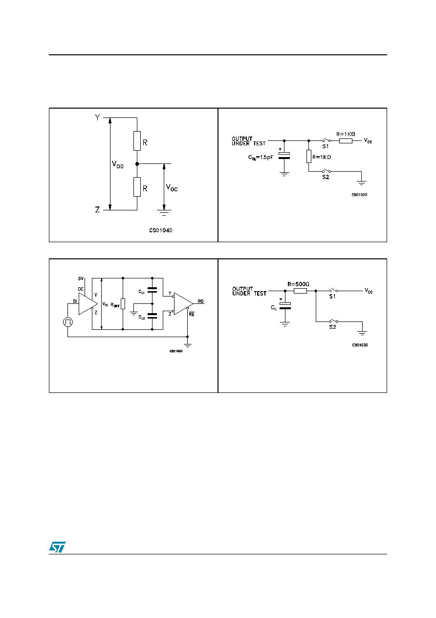
Figure 2.
Driver DC test load
Figure 3.
Receiver timing test load
Figure 4.
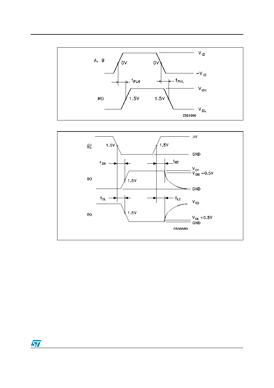
Drive/receiver timing test circuit
Figure 5.
Driver timing test load
Test circuit and typical characteristics
ST485
10/19
Figure 6.
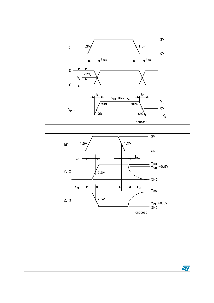
Driver propagation delay
Figure 7.
Driver enable and disable time
ST485
Test circuit and typical characteristics
11/19
Figure 8.
Receiver propagation delay
Figure 9.
Receiver Enable and Disable Time
Test circuit and typical characteristics
ST485
12/19
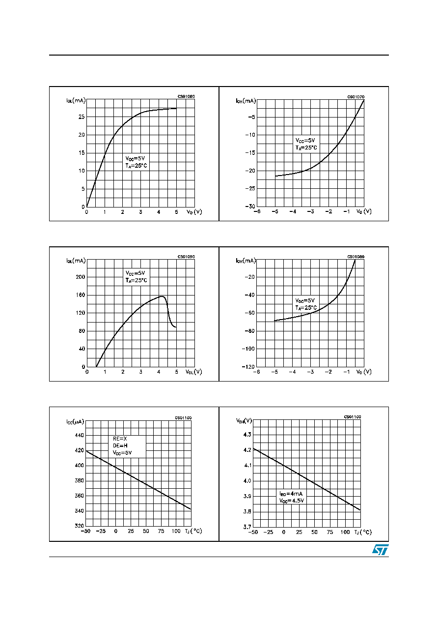
Figure 10.
Receiver output current vs. output
low voltage
Figure 11.
Receiver output current vs. output
high voltage
Figure 12.
Driver output current vs. output low
voltage
Figure 13.
Driver output current vs. output
high voltage
Figure 14.
Supply current vs. temperature
Figure 15.
Receiver high level output voltage
vs. temperature
ST485
Test circuit and typical characteristics
13/19
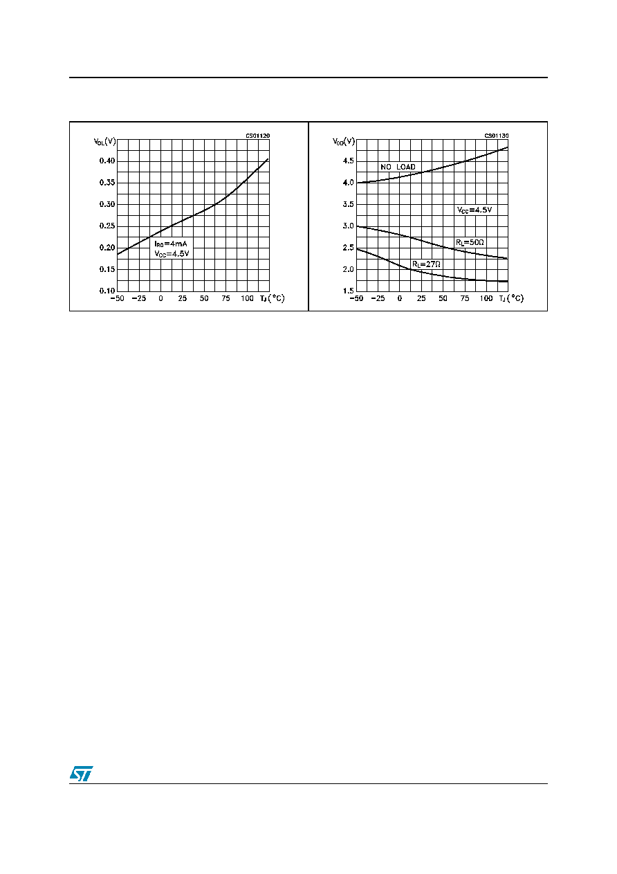
Figure 16.
Receiver low level output voltage
vs. temperature
Figure 17.
Differential driver output voltage
vs. temperature

Package mechanical data
ST485
14/19
6 Package
mechanical
data
In order to meet environmental requirements, ST offers these devices in ECOPACKÆ
packages. These packages have a Lead-free second level interconnect. The category of
second level interconnect is marked on the package and on the inner box label, in
compliance with JEDEC Standard JESD97. The maximum ratings related to soldering
conditions are also marked on the inner box label. ECOPACK is an ST trademark.
ECOPACK specifications are available at:
www.st.com
ST485
Package mechanical data
15/19
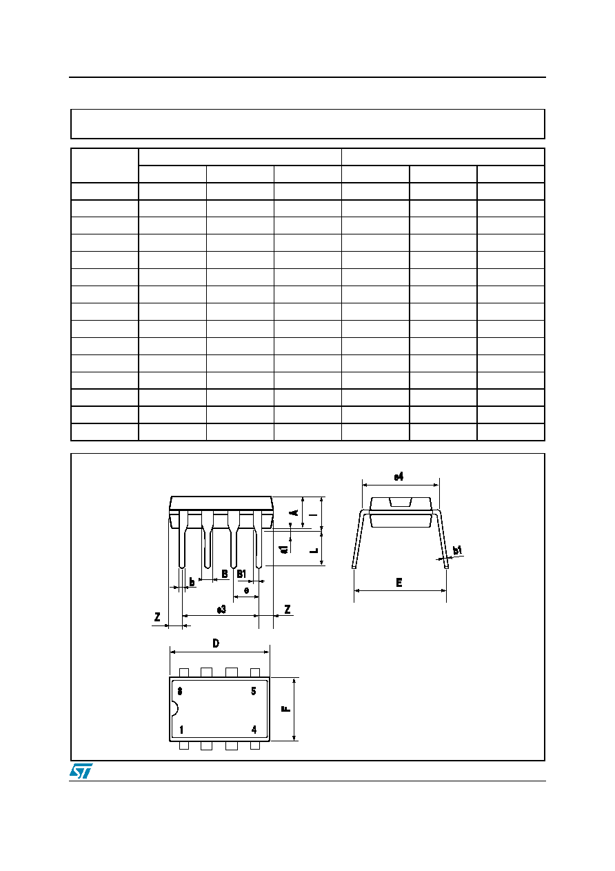
DIM.
mm.
inch
MIN.
TYP
MAX.
MIN.
TYP.
MAX.
A
3.3
0.130
a1
0.7
0.028
B
1.39
1.65
0.055
0.065
B1
0.91
1.04
0.036
0.041
b
0.5
0.020
b1
0.38
0.5
0.015
0.020
D
9.8
0.386
E
8.8
0.346
e
2.54
0.100
e3
7.62
0.300
e4
7.62
0.300
F
7.1
0.280
I
4.8
0.189
L
3.3
0.130
Z
0.44
1.6
0.017
0.063
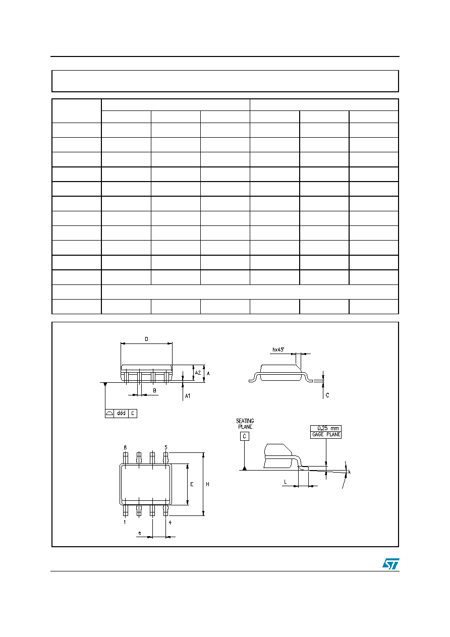
Plastic DIP-8 MECHANICAL DATA
P001F
Package mechanical data
ST485
16/19
DIM.
mm.
inch
MIN.
TYP
MAX.
MIN.
TYP.
MAX.
A
1.35
1.75
0.053
0.069
A1
0.10
0.25
0.04
0.010
A2
1.10
1.65
0.043
0.065
B
0.33
0.51
0.013
0.020
C
0.19
0.25
0.007
0.010
D
4.80
5.00
0.189
0.197
E
3.80
4.00
0.150
0.157
e
1.27
0.050
H
5.80
6.20
0.228
0.244
h
0.25
0.50
0.010
0.020
L
0.40
1.27
0.016
0.050
k
∞ (max.)
ddd
0.1
0.04
SO-8 MECHANICAL DATA
0016023/C
8
ST485
Package mechanical data
17/19
DIM.
mm.
inch
MIN.
TYP
MAX.
MIN.
TYP.
MAX.
A
330
12.992
C
12.8
13.2
0.504
0.519
D
20.2
0.795
N
60
2.362
T
22.4
0.882
Ao
8.1
8.5
0.319
0.335
Bo
5.5
5.9
0.216
0.232
Ko
2.1
2.3
0.082
0.090
Po
3.9
4.1
0.153
0.161
P
7.9
8.1
0.311
0.319
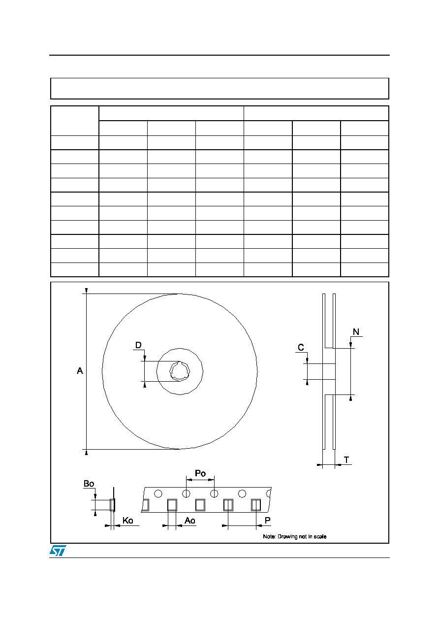
Tape & Reel SO-8 MECHANICAL DATA

Revision history
ST485
18/19
7 Revision
history
Table 8.
Revision history
Date
Revision
Changes
21-Mar-2006
12
Order codes has been updated and new template.

ST485
19/19
Please Read Carefully:
Information in this document is provided solely in connection with ST products. STMicroelectronics NV and its subsidiaries ("ST") reserve the
right to make changes, corrections, modifications or improvements, to this document, and the products and services described herein at any
time, without notice.
All ST products are sold pursuant to ST's terms and conditions of sale.
Purchasers are solely responsible for the choice, selection and use of the ST products and services described herein, and ST assumes no
liability whatsoever relating to the choice, selection or use of the ST products and services described herein.
No license, express or implied, by estoppel or otherwise, to any intellectual property rights is granted under this document. If any part of this
document refers to any third party products or services it shall not be deemed a license grant by ST for the use of such third party products
or services, or any intellectual property contained therein or considered as a warranty covering the use in any manner whatsoever of such
third party products or services or any intellectual property contained therein.
UNLESS OTHERWISE SET FORTH IN ST'S TERMS AND CONDITIONS OF SALE ST DISCLAIMS ANY EXPRESS OR IMPLIED
WARRANTY WITH RESPECT TO THE USE AND/OR SALE OF ST PRODUCTS INCLUDING WITHOUT LIMITATION IMPLIED
WARRANTIES OF MERCHANTABILITY, FITNESS FOR A PARTICULAR PURPOSE (AND THEIR EQUIVALENTS UNDER THE LAWS
OF ANY JURISDICTION), OR INFRINGEMENT OF ANY PATENT, COPYRIGHT OR OTHER INTELLECTUAL PROPERTY RIGHT.
UNLESS EXPRESSLY APPROVED IN WRITING BY AN AUTHORIZE REPRESENTATIVE OF ST, ST PRODUCTS ARE NOT DESIGNED,
AUTHORIZED OR WARRANTED FOR USE IN MILITARY, AIR CRAFT, SPACE, LIFE SAVING, OR LIFE SUSTAINING APPLICATIONS,
NOR IN PRODUCTS OR SYSTEMS, WHERE FAILURE OR MALFUNCTION MAY RESULT IN PERSONAL INJURY, DEATH, OR
SEVERE PROPERTY OR ENVIRONMENTAL DAMAGE.
Resale of ST products with provisions different from the statements and/or technical features set forth in this document shall immediately void
any warranty granted by ST for the ST product or service described herein and shall not create or extend in any manner whatsoever, any
liability of ST.
ST and the ST logo are trademarks or registered trademarks of ST in various countries.
Information in this document supersedes and replaces all information previously supplied.
The ST logo is a registered trademark of STMicroelectronics. All other names are the property of their respective owners.
© 2006 STMicroelectronics - All rights reserved
STMicroelectronics group of companies
Australia - Belgium - Brazil - Canada - China - Czech Republic - Finland - France - Germany - Hong Kong - India - Israel - Italy - Japan -
Malaysia - Malta - Morocco - Singapore - Spain - Sweden - Switzerland - United Kingdom - United States of America
www.st.com